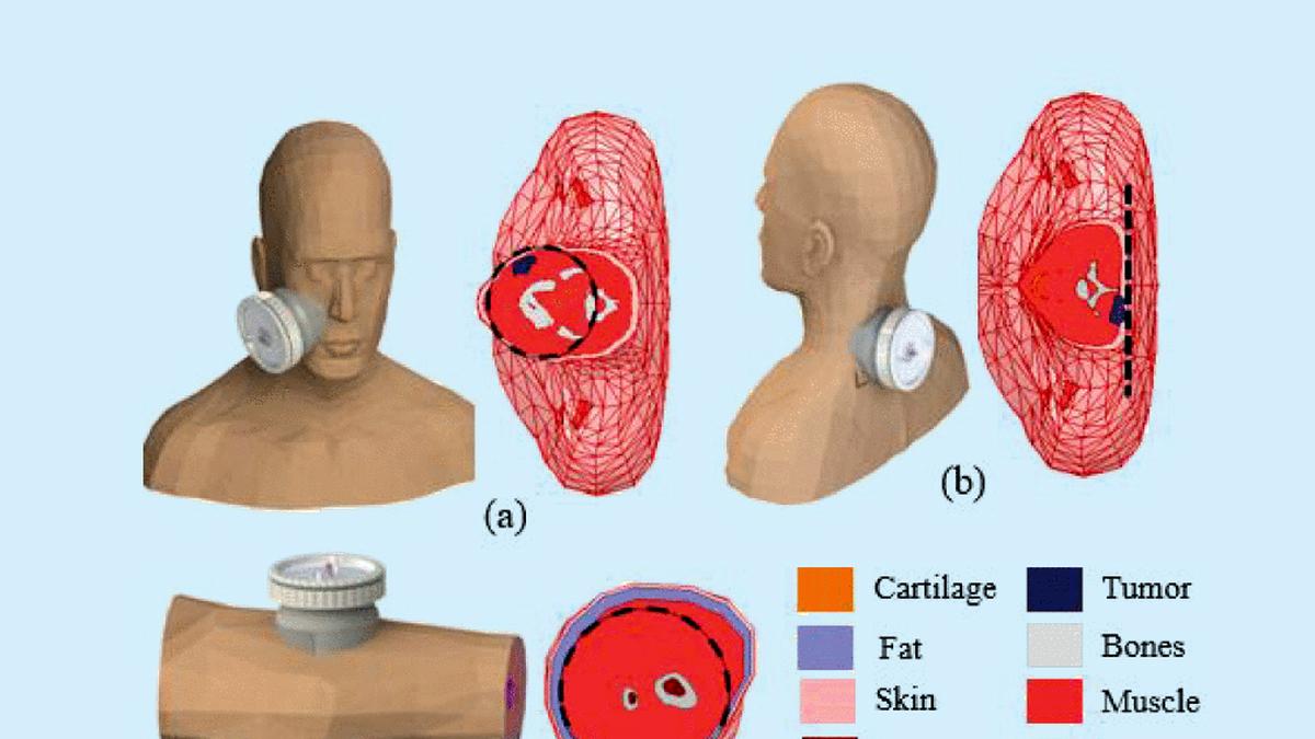
Cancer treatments like radiation and chemotherapy are powerful because they target and destroy cancer cells that other methods cannot reach. Yet, doctors often use an additional treatment after these — called adjuvant therapy — to eliminate any remaining cancer cells. One such promising adjuvant treatment is hyperthermia therapy, which uses heat to make tumours more sensitive to radiation and chemotherapy.
In hyperthermia treatment, doctors raise the temperature of the tumour to about 40–44 degree C for up to an hour. This weakens cancer cells while leaving healthy tissue relatively unharmed. It works especially well for superficial cancers — those on or near the body’s surface, such as cancers of the breast, neck, or skin.
However, heating small, curved areas of the body — like the face or nose — poses a major challenge. Existing hyperthermia devices are too large and often fail to deliver heat evenly to small, localised tumours.
To solve this, Rahul Choudhury and Prof Kavita Arunachalam, at the Department of Engineering Design at IIT-Madras, have developed a compact hyperthermia applicator that operates at 434 MHz, a frequency used for cancer treatment. Their design features a single small antenna with an integrated water bolus — a thin, water-filled layer that helps the device conform perfectly to curved surfaces and ensures even heating without air gaps.
Tests conducted on artificial tissue models and real chicken and bovine samples showed highly efficient heating, with over 96 per cent power coupling and stable, targeted energy delivery. The device is significantly smaller than current models and offers a way to treat small, localised tumours that were previously difficult to reach.
Diamond in quantum sensor
Under the National Quantum Mission (NQM) of the Department of Science and Technology (DST), researchers at IIT-Bombay’s PQuest Group have built India’s first quantum diamond microscope (QDM) — a device that can capture magnetic fields in real time at the microscopic level. This marks a major step for the country in the field of quantum sensing and has earned its first patent in this area.
Formally announced at the Emerging Science Technology and Innovation Conclave (ESTIC 2025), the QDM has exciting potential in neuroscience, materials research, and non-destructive testing of semiconductor chips. It can map magnetic fields across multiple 3D layers inside an encapsulated chip, making it a powerful tool for the semiconductor industry.
Developed by a team led by Prof Kasturi Saha, the QDM is based on nitrogen-vacancy (NV) centres in diamonds — tiny atomic defects that make diamonds extremely sensitive to changes in magnetic, electric, and thermal fields. The NV centres use light to detect magnetic fields through a process called optically detected magnetic resonance (ODMR). By creating a thin diamond layer rich in NV centres, the QDM can perform widefield imaging of magnetic activity, much like a high-resolution optical microscope.
As electronic devices move toward 3D chip designs, traditional diagnostic tools can no longer ‘see’ inside complex, multi-layer circuits. The QDM solves this challenge by offering direct, high-resolution 3D magnetic mapping of chips, batteries, and microelectronic systems.
Prof Saha’s team now plans to combine the QDM with AI and machine learning to create a next-generation imaging platform for chip diagnostics, biological imaging, and geological magnetic studies — all enabled by precise, 3D magnetic field visualisation.
More Like This
Published on November 17, 2025
