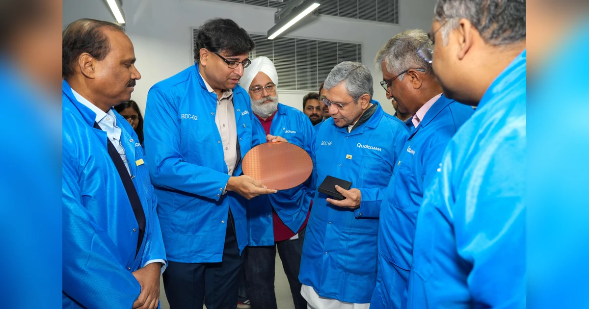
Qualcomm has completed the tape-out of a 2nm chip design, marking a new milestone for advanced semiconductor work being carried out from India. The company said the design work was done across its engineering centres in Bengaluru, Chennai and Hyderabad, underlining the growing role of India in global chip development at a time when the government is pushing to expand the country’s semiconductor ecosystem under the India Semiconductor Mission 2.0.
The announcement comes as India is trying to build deeper capabilities in chip design, packaging, testing and, eventually, manufacturing. While the 2nm chip will not be manufactured in India, the tape-out signals that Indian engineering teams are now involved in some of the most advanced stages of chip design work.
What Qualcomm announced and what ‘tape-out’ means
In semiconductor development, “tape-out” refers to the stage at which a chip’s design is finalised and sent to a foundry for manufacturing. It marks the end of the design phase and the point at which the layout data is prepared for fabrication. After tape-out, the chip moves into production, followed by testing and validation before it can be used in products.
Qualcomm said it has successfully taped out a 2nm chip design, which places the work at the cutting edge of current semiconductor technology. The “2nm” label refers to an advanced manufacturing node, used as a shorthand for higher transistor density, improved power efficiency and better performance compared to older nodes. Chips at this level are also significantly more complex and expensive to design, requiring advanced tools, large engineering teams and long development cycles.
It is important to note that a tape-out is a design milestone, not the start of manufacturing in India. The actual fabrication of such advanced chips is still handled by a small number of global foundries. The significance, in this case, lies in the fact that the design work is being carried out from India.
In a statement, Union minister of Railways, Information & Broadcasting, and Electronics & IT, Ashwini Vaishnaw said India is increasingly becoming a centre for advanced semiconductor design work. He said, “Seeing Qualcomm’s work here, its engineering strength, deep design capabilities, and long-standing commitment to India, is truly impressive. Milestones like this demonstrate how far India’s design ecosystem has come and align strongly with our vision of building a globally competitive semiconductor industry”.
Qualcomm, for its part, said the tape-out reflects the role its engineering teams in India play across design, validation and system-level development as part of its global chip programmes.
“Qualcomm’s R&D centres in India are contributing across multiple layers of system design, from architecture to implementation, software platforms, and use-case optimisation,” said Shashi Reddy, Senior Vice President, Engineering, Qualcomm India Private Limited.
How this fits into India’s semiconductor push
The announcement also comes against the backdrop of the government’s semiconductor programme, which has been expanded under India Semiconductor Mission (ISM) 2.0 in the Union Budget 2026–27. Under ISM 1.0, approved in 2021, the government put in place an incentive framework of Rs 76,000 crore to support silicon fabs, compound semiconductor units, assembly and testing facilities, and chip design companies.
As of December 2025, the government has approved 10 projects across six states with a total investment of about Rs 1.60 lakh crore. These include a Micron assembly and test facility in Gujarat, Tata Electronics’ fabrication and packaging projects in Gujarat and Assam, a joint venture involving CG Power, Renesas and STARS Microelectronics, as well as projects from companies such as Kaynes Technology, SiCSem and others focused on packaging, testing and specialised manufacturing.
Alongside manufacturing and packaging, the Design Linked Incentive (DLI) scheme has focused on strengthening India’s chip design base. According to government data, the programme supports two dozen design startups, has enabled multiple tape-outs from both startups and academic institutions, and has facilitated access to advanced design tools through a national EDA platform.
ISM 2.0 builds on this by shifting more focus towards equipment, materials, full-stack design capabilities and a longer-term roadmap that includes advanced nodes such as 3nm and 2nm. For 2026–27, the modified semiconductor programme has an outlay of Rs 8,000 crore, with targets spanning new fab investments, packaging and testing units, and additional support for design companies. As part of it, India also plans to achieve the capability to design and manufacture chips required for nearly 70–75 per cent of domestic applications by 2029.
Why this matters for India
Semiconductors are now central to sectors ranging from consumer electronics and telecom to automobiles, industrial systems and defence. Recent global supply disruptions have highlighted how dependent economies are on a small number of electronics component producing regions. For India, the stated goal has been to reduce reliance on imports over time and build a more resilient domestic ecosystem across design, manufacturing and packaging.
In the near term, design remains India’s strongest link in the semiconductor value chain. Large global chip companies already run substantial engineering operations in the country, and Indian teams are involved in architecture, verification, software and system-level work for products that are eventually manufactured elsewhere. A 2nm tape-out adds to that picture by showing that work from India is not limited to mature nodes, but also extends to advanced designs that sit at the top end of the industry’s technology roadmap.
Interest from other chipmakers
Qualcomm is not the only company looking at India more closely as part of its semiconductor strategy. According to a report by The Times of India, Taiwanese chipmaker MediaTek has said it is open to getting chips manufactured in India, as the country builds out its semiconductor infrastructure and offers incentives under the government’s programme.
While large-scale manufacturing at advanced nodes remains a longer-term objective, such statements point to growing interest from global chip companies in engaging with India not just as a design base, but also as a potential part of the manufacturing and supply chain ecosystem over time.
